Introduction
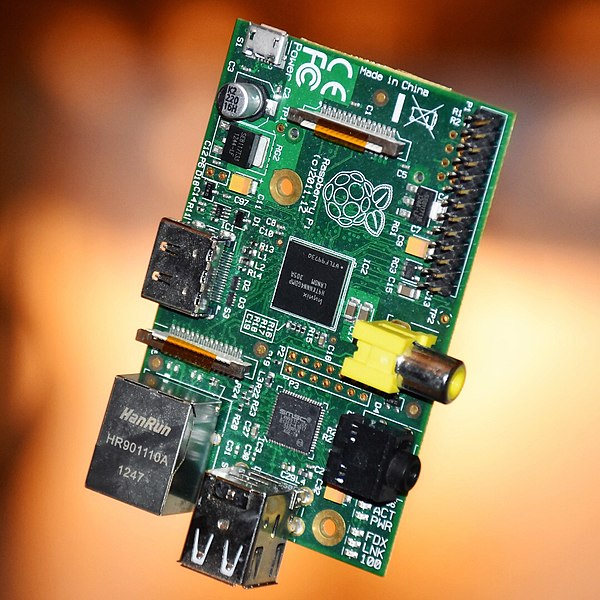
Today, anything with electronic components is sure to have a printed circuit board (PCB) — from TVs and coffee machines, to cars and even CT scanners. Because of this ubiquity, the global PCB industry is predicted to be worth $69.5 billion (€58.8 billion) by 2024, with a compound annual growth rate of 4-6%.
But how did the use of these small yet immensely powerful pieces of tech become this widespread? What’s in store for the technology in the future? This brief history of PCB technology may hold the answers.
The 20th Century
It all began when German inventor Albert Hanson patented a design for a multi-layered insulation board in 1903. It had a flat foil conductor, technically making it the PCB’s first predecessor. He had intended to use it for through-hole application, a method still used today, which involved punching a hole through two layers of the board and establishing an electrical connection using perpendicular wires.
Progress continued until 1925, when Charles Ducas patented a process to add conductive inks to the insulating material. This paved the way for the “printed” component of the PCB.
However, major advancements weren’t made until World War II, when Paul Fisler, an Austrian living in the UK, created the first operational printed board, and even made a radio with it in 1943. Eventually, the Brits shared this design with Americans, who perfected the manufacturing process for use in the military.
The Early Computer Age
Two decades later, electronic devices became more widely used thanks to PCBs, but the boards themselves were still not available commercially. However, the technology continued to develop, and eventually became more sophisticated during the US and Russia’s famed space race. In particular, IBM introduced surface mount technology, so more components could be placed on a PCB. Meanwhile, the Hazeltine Corporation patented plated through-hole technology, ensuring components wouldn’t have any crossover connections.
PCBs soon reached the public market in the ’70s and ’80s. During this time, the use of consumer electronics increased, with the VHS, cameras, and video game consoles all entering the mainstream. This meant PCBs were more in-demand than ever before — but they were still being designed by hand. Thankfully, living in the computer age meant developers eventually introduced PCB layout design software to streamline the manufacturing process. Using this software, designers could now use the latest routing tools, establish design rules, and verify power and signal distributions on multiple boards simultaneously. With these integrated systems, manufacturers could essentially just feed text files to machines, which would then print the boards.
Recent Years
Finally, PCBs have become increasingly miniaturized in the last few decades thanks to the ball grid array — a type of chip carrier used to more easily mount components.
Additionally, with the manufacturing of smaller electronics and equally smaller components, people abandoned hand-soldering and became more reliant on software to manufacture PCBs. And today, we can cheaply mass-produce PCBs that are even more powerful and durable, despite their small size.
Aside from using SMT tech, however, many other fabrication and leverage techniques help make modern PCBs more accessible. In particular, PCB designers often refer to the live drill table — a chart that contains information on hole sizes to hole tolerances, among other things. It was created due to a delay in production caused by the resubmission of drill data and is commonly integrated into modern PCB design software.
Where is PCB Technology Today?
As of late, it can sometimes feel like technology has been advancing far too quickly. But, as we previously discussed here on the Automated Podcast, it’s all just Moore’s Law, and computation capacity will probably increase by up to 100x in the next decade. So, whether they’re increasingly used in advanced robotics or the continuing miniaturization of consumer electronics, PCB adoption can only become more widespread in the coming years.